- Ordering of layers in an ultra-thin film [3]
- Thickness of layers [1-3]
- Distribution of elements and chemical states within the film (depth profile reconstruction) [3]

Angle Resolved XPS

Technique Overview
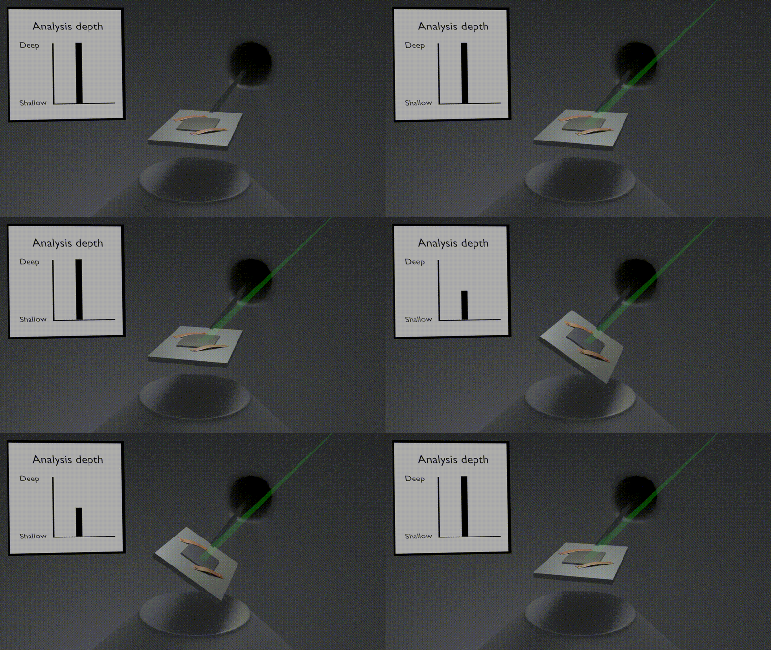
Not to be confused with Angle-resolved photoemission spectroscopy (ARPES), angle-resolved XPS (ARXPS) is a technique which varies the emission angle at which the electrons are collected and in doing so, enabling electron detection from different depths by exploiting the inelastic mean free path (IMFP) of the photoelectrons.
Applications and Fields
- Thin film analysis
- Thickness analysis
- Self-assembled monolayers / orientation analysis
- Analysis of terminating layers

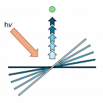
Figure 1. Simple illustration of an ARXPS measurement of a silicon oxide layer on a silicon wafer. Note how at the more grazing angle, the top most oxide (and the sub-oxides) are more prominant as we are now more surface sensitive
ARXPS measurements are realtively simple to perform. XPS data is collected at a series of angles, typically from 0° to 75° photoemission angle. Five or six angles are usually sufficient and Cumpson [2] has recommended acquiring data at 0°, 40°, 55°, 63° and 70° for materials such as polymers which exhibit weak elastic scattering, and 0°, 33°, 45°, 54°, 60° for samples containing elements of larger atomic number (e.g. an iron alloy), where elastic scattering is stronger. Performing measurements at these angles concentrates the data acquisition at the higher photoemission angles, where the analysis is most sensitive to the sample surface.
The principal behind why we see a change in the surface sensitivity arises from the change in effective attenuation length when we revolve a sample around it’s axis.
If we think of our general equation for determining the attenuation length of an electron within a sample, we have a parameter which determines the amount of radiation which is reduced as a result of passing Δx thickness of a sample.
μ = lim (Δx → 0) (1 – (I / I0) / Δx
Where μ = the attenuation coefficient
I = intensity of radiation following transmission
I0 = intensity of incident radiation
Attenuation length is then determined from the reciprocal of this.
λ = 1/μ
And gives us a general equation for attenuation (of radiation OR electrons)
I/I0 = exp(-Δx/λ)
When we revolve our sample, we are increasing the effective path length from the point of photoelectron emission – to the material surface, and hence our Δx value – so we will be reducing the intensity of our I for those electrons that originate deeper within the material. The end result of this is that our eventual spectrum is more representative of the atoms from closer to the surface.
ARXPS involves analysing data from a sample at different angles, and identifying the changes that arise as a result of this change in surface sensitivity – outlined in the previous section.
Software for Quantitative ARXPS and ARAES
Determination of Surface Nano-structures by analysis of angle resolved XPS or AES
Includes facilities for
- Three different ways to normalize the data (with or without reference spectra)
- Flexible adjustment of concentration and coverage for each layer
- Elastic scattering correction by the recent algorithm of Nefedov
- User friendly data handling
- Graphical user interface
- Automatic optimization of structure to data set
Possibly the simplest application of ARXPS is for highlighting chemical and electronic differences between the ‘near-surface’ and ‘outer-surface’ of a material.
Analysis of a material at the ‘flat’ angle (0° rotation) and a ‘steep’ rotation (60-75° rotation) permits separation of the chemical environment from the very outer surface, versus the standard XPS information depth (near-surface).

By monitoring the changing intensity of a substrate peak as a function of analysis angle, provided the inelastic mean free path / attenuation depth is known – it is possible to calculate the thickness of a film or overlayer on a flat surface using ARXPS.
Is = Is0.exp(-d/λs(o).cos(θ)
Where:
Is = Intensity of the substrate signal following attenuation through the overlayer
Is0 = Intensity of the substrate signal before attenuation through the overlayer
d = film thickness
λs(o) = IMFP of substrate electrons, through overlayer material
θ = Take off angle
Is0 is unknown, but with multiple analysis angles, you may determine this either through graphical means, or using simultaneous equations to cancel down.

Figure 1. Simple illustration of an ARXPS measurement of a silicon oxide layer on a silicon wafer. Note how at the more grazing angle, the top most oxide (and the sub-oxides) are more prominant as we are now more surface sensitive
ARXPS measurements are realtively simple to perform. XPS data is collected at a series of angles, typically from 0° to 75° photoemission angle. Five or six angles are usually sufficient and Cumpson [2] has recommended acquiring data at 0°, 40°, 55°, 63° and 70° for materials such as polymers which exhibit weak elastic scattering, and 0°, 33°, 45°, 54°, 60° for samples containing elements of larger atomic number (e.g. an iron alloy), where elastic scattering is stronger. Performing measurements at these angles concentrates the data acquisition at the higher photoemission angles, where the analysis is most sensitive to the sample surface.
The principal behind why we see a change in the surface sensitivity arises from the change in effective attenuation length when we revolve a sample around it’s axis.
If we think of our general equation for determining the attenuation length of an electron within a sample, we have a parameter which determines the amount of radiation which is reduced as a result of passing Δx thickness of a sample.
μ = lim (Δx → 0) (1 – (I / I0) / Δx
Where μ = the attenuation coefficient
I = intensity of radiation following transmission
I0 = intensity of incident radiation
Attenuation length is then determined from the reciprocal of this.
λ = 1/μ
And gives us a general equation for attenuation (of radiation OR electrons)
I/I0 = exp(-Δx/λ)
When we revolve our sample, we are increasing the effective path length from the point of photoelectron emission – to the material surface, and hence our Δx value – so we will be reducing the intensity of our I for those electrons that originate deeper within the material. The end result of this is that our eventual spectrum is more representative of the atoms from closer to the surface.
Surface roughness may be indirectly probed by ARXPS – by way of observing peak broadening, inconsistent compositional dependence on angle, or by comparisons with a known flat surface.
-
References
[1] R.W. Paynter, An ARXPS primer, J. Electro. Spec. and Relat. Phenom., 169 (2009) 1-9. Read the paper here: https://doi.org/10.1016/j.elspec.2008.09.005
[2] P. J. Cumpson, Angle-reolved XPS and AES: depth-resolution limits and a general comparison of properties of depth-profile reconstruction method, J. Electro. Spec. and Relat. Phenom., 73(1995) 25-52. Read the paper here: https://doi.org/10.1016/0368-2048(94)02270-4
[3] C.R.Brundle, G. Conti, P. Mack, XPS and angle resolved XPS, in the semiconductor industry: Characterization and metrology control of ultra-thin films, J. Electro. Spec. and Relat. Phenom., 178-179 (2010) 433-448. Read the paper here: http://doi.org/10.1016/j.elspec.2010.03.008